Device interfaces
PDM microphone inputs
Two standard PDM MEMS microphones should be connected to the MIC_DATA pin. The data input makes use of the left and right channel output capability of standard MEMS microphones and the microphone data is read on alternative edges of the MIC_CLK signal. The XVF3610 reads one microphone on the positive edge of the microphone clock and the other microphone on the negative edge of the clock.
The XVF3610 outputs a microphone clock at 3.072MHz on the MIC_CLK output, which must be fed directly to both microphones. This signal must be used to clock the microphone PDM output to avoid undefined artefacts in the processed audio stream. One microphone should be set to be left (output on rising edge of clock) and the other right (output on the falling edge of clock).
An example microphone circuit is shown in the figure below:
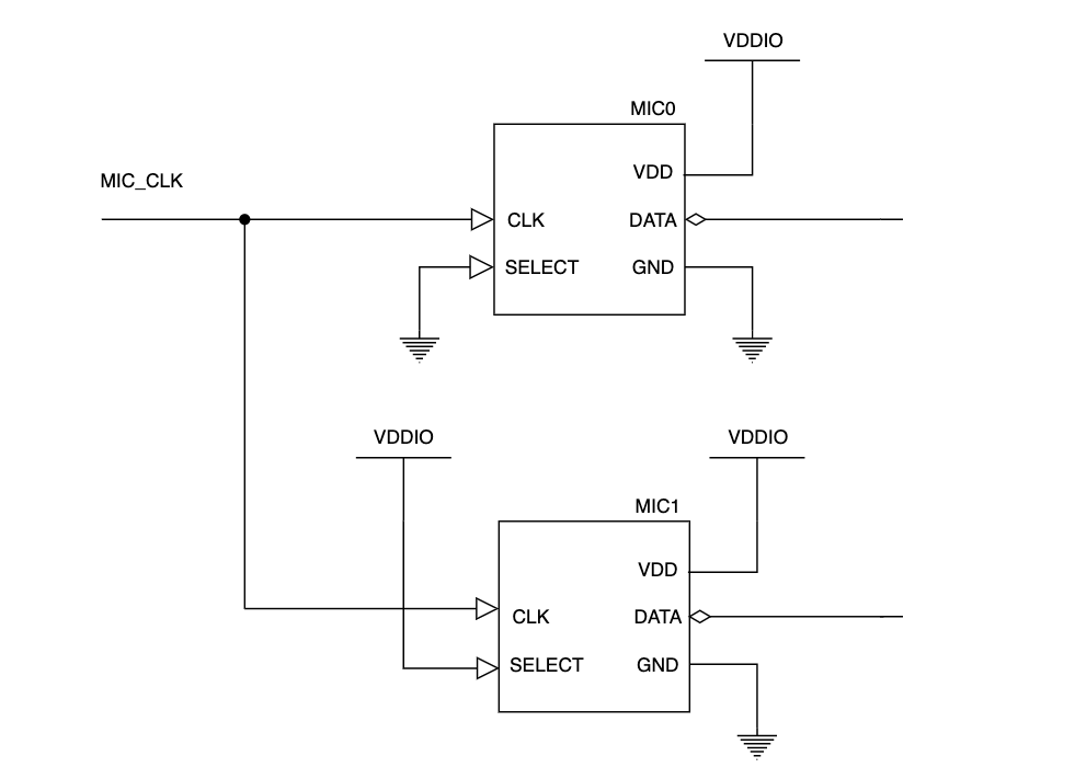
Fig. 13 PDM microphone schematic
The voice processor has been tested and characterised with microphones placed with a 71mm separation and connected to the product enclosure in such a way that the acoustic path to each microphone from outside the product is independent. The XVF3610 algorithms automatically adapt to alternative spacing, but differences in audio performance may occur and should be thoroughly characterised.
QSPI Boot mode
When QSPI boot mode is enabled (default), the XVF3610 enables the six QSPI pins, see table below, and drives the QSPI clock as a QSPI Master. A READ command is issued with a 24-bit address 0x000000.
Signal |
Des cription |
Comment |
P i n |
I / O |
|---|---|---|---|---|
QSPI_CS_N |
QSPI Chip Select |
Pull high externally to the device using a 4.7k ohm resistor |
3 |
O |
QSPI_CL K/SPI_CLK |
QSPI Clock |
5 |
O |
|
QSPI_D0 |
QSPI Data Line 0 |
5 9 |
I / O |
|
QSPI_D 1/BOOTSEL |
QSPI Data Line 1 and boot se lection. |
If pin is tied high via a 4.7k ohm resistor on startup, the device will start in SPI slave boot mode. If the pin is left floating, pulled low or connected to a quad SPI D1 pin on a memory device, the device will start in QSPI master mode and attempt to boot from a local QSPI flash memory. |
1 |
I / O |
QSPI_D2 |
QSPI Data Line 2 |
6 0 |
I / O |
|
QSPI_D3 |
QSPI Data Line 3 |
2 |
I / O |
The XVF3610 expects each byte to be transferred with the least-significant nibble first. Programmers that write bytes into a QSPI interface using the most significant nibble first may have to reverse the nibbles in each byte of the image stored in the QSPI device. When bulk programming flash devices the Quad Enable bit in the flash setting register should be set.
For further information about the boot sequence refer to the XU316-1024-QF60(A/B) datasheet.
SPI Interface
The SPI interface can be utilised in both Master and Slave configurations for peripheral control of components like DACs and ADCs (Master), and SPI boot from host a host processor (Slave).
Peripheral component control
Once the XVF3610 has successfully booted, the SPI interface can be used to configure peripheral components such as DACs, ADCs and keyword detection devices. In this mode the SPI interface operates as a master, and transfers data held in flash, or received from the host over the control interface. The interface operates with the following specifications:
1MHz SPI clock
Up to 128 bytes SPI write
Up to 56 bytes SPI read
For further information on this configuration consult the User Guide.
SPI slave boot
To enable the SPI boot from an external host processor, the QSPI_D1/BOOTSEL should be pulled to VDDIO on power-up. This activates the SPI interface, which operates as a slave to the host processor for the transfer of the boot image, which is clocked in with the least significant bit first in each transferred byte.
This is an alternative to using an attached QSPI flash to automatically transfer boot data on start-up.
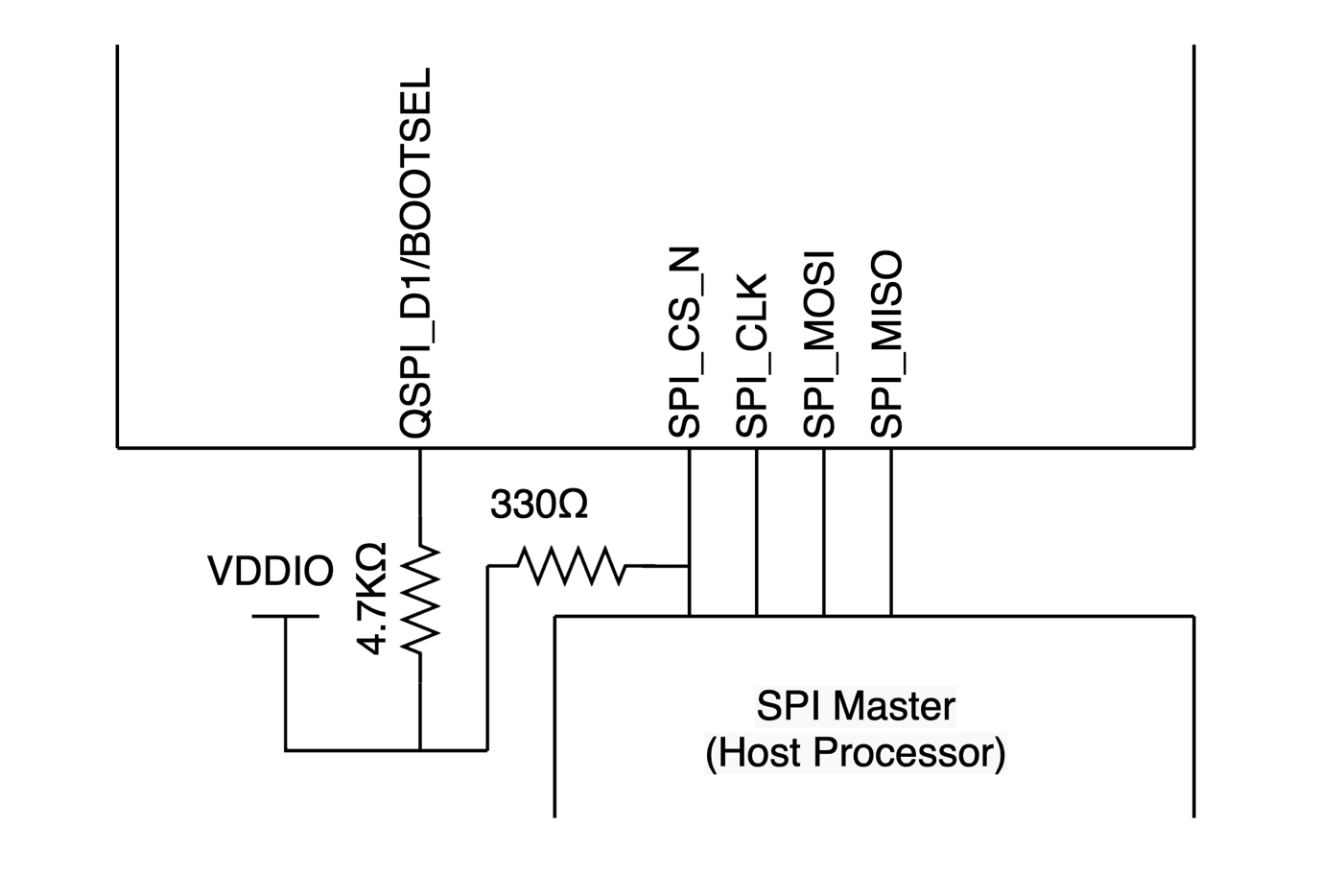
Fig. 14 XVF3610 SPI slave boot configuration
The SPI pins are shown below in the table below.
S ignal |
Description |
Comment |
P i n |
I / O |
|---|---|---|---|---|
SP I_CLK |
SPI Clock |
5 |
I |
|
SPI _CS_N |
SPI Chip Select |
Pull high externally to the device using a 4.7k ohm resistor |
6 |
I |
SPI _MOSI |
SPI Master Out Slave In |
7 |
I |
|
SPI _MISO |
SPI Master In Slave Out |
May be left floating if not required |
4 7 |
O |
Integrated USB interface
USB Audio Class 1.0 running at Full Speed (12Mbps) is used to deliver processed voice audio to the host processor, stereo reference audio from the host and as a control interface. In this mode the adaptive USB Audio endpoint is used to generate an MCLK synchronised to the USB host. This is driven out of MCLK
Name |
Description |
P i n |
|---|---|---|
USB_DP |
Connect to USB connector |
2 9 |
USB_DM |
Connect to USB connector |
2 8 |
US B_VBUS_DET |
Do not connect Self-powered operation is not supported by current device firmware |
4 3 |
USB_VDD18 |
1.8V supply for USB-PHY - May be left floating if the USB interface is not used. |
3 1 |
USB_VDD33 |
3.3V supply to the USB-PHY May be left floating if the USB interface is not used. |
3 0 |
The table below shows the signals required to implement a USB interface using the XVF3610.
Note
Currently the -UA firmware only supports use in a bus powered configuration
I2S Audio Interface
The XVF3610 operates as an I2S slave outputting audio to the host processor and receiving reference audio signal. This bidirectional flow of audio samples must be synchronised to a single set of I2S clocks, see Table below:
Signal |
Description |
Comment |
P i n |
I / O |
|---|---|---|---|---|
MCLK |
Master audio clock |
1 4 |
I |
|
I2S_BCLK |
I2S bit sy nchronisation clock |
Configurable for 16KHz (1.024MHz) and 48KHz (3.072MHz) sample rates |
1 3 |
I |
I2S_LRCK |
I2S Left/Right clock |
48kHz or 16KHz clock derived as I2S_BLCK/64. |
1 0 |
I |
I2S_DIN |
I2S Data In |
Reference audio data from I2S device |
5 3 |
I |
I2S_DOUT |
I2S Data Out |
Audio data out to host processor |
9 |
O |
The I2S audio samples are transmitted serially with a one I2S_BCLK delay between the change of I2S_LRCK phase and the start (MSB) of the audio sample for that channel. This the standard alignment for I2S systems.
I2C Control interface
The I2C Slave interface is used to control and configure the parameters on the XVF3610.
Warning
I2C commands received prior to I2S clocks being activated will not be processed and may result in undefined behaviour. Therefore, it is important to ensure that the I2S interface is activated before parameterisation of the device is undertaken.
The interface operates with the following specifications:
100 kbps SCL clock speed
Register read/write
Up to 56 byte I2C read/write
For more information on control and configuration of the XVF3610 please refer to the User Guide.
The device I2C address is 0x2C, and the pin connections are shown below.
Si gnal |
Description |
C omment |
P i n |
I / O |
|---|---|---|---|---|
I2C _SCL |
I2C serial clock line for receiving control command from I2C host |
4 4 |
I / O |
|
I2C _SDA |
I2C serial data line for receiving control command from I2C host |
4 5 |
I / O |
General Purpose Input/Output
Four input and four output pins are provided to allow general-purpose I/O such as LEDs and button controls. Input pins can be individually read by the host using the control interface and configured to detect edge events. The output pins can be individually set, and they have configurable Pulse Width Modulated (PWM) brightness control with blinking sequences.
The GPIO pins are shown in the table below.
Name |
Description |
Pin |
I/O |
|---|---|---|---|
IP_0 |
General purpose input |
46 |
I |
IP_1 |
General purpose input |
50 |
I |
IP_2 |
General purpose input |
48 |
I |
IP_3 |
General purpose input |
51 |
I |
OP_0 |
General purpose output |
40 |
O |
OP_1 |
General purpose output |
54 |
O |
OP_2 |
General purpose output |
55 |
O |
OP_3 |
General purpose output |
56 |
O |
For more information on configuring these inputs and outputs, please refer to the User Guide.