Pin diagram
Pin configuration
The pinout of the XVF3610, including all optional interfaces, is shown in the figure below.
Pins marked RESVD are internally connected and should remain unconnected.
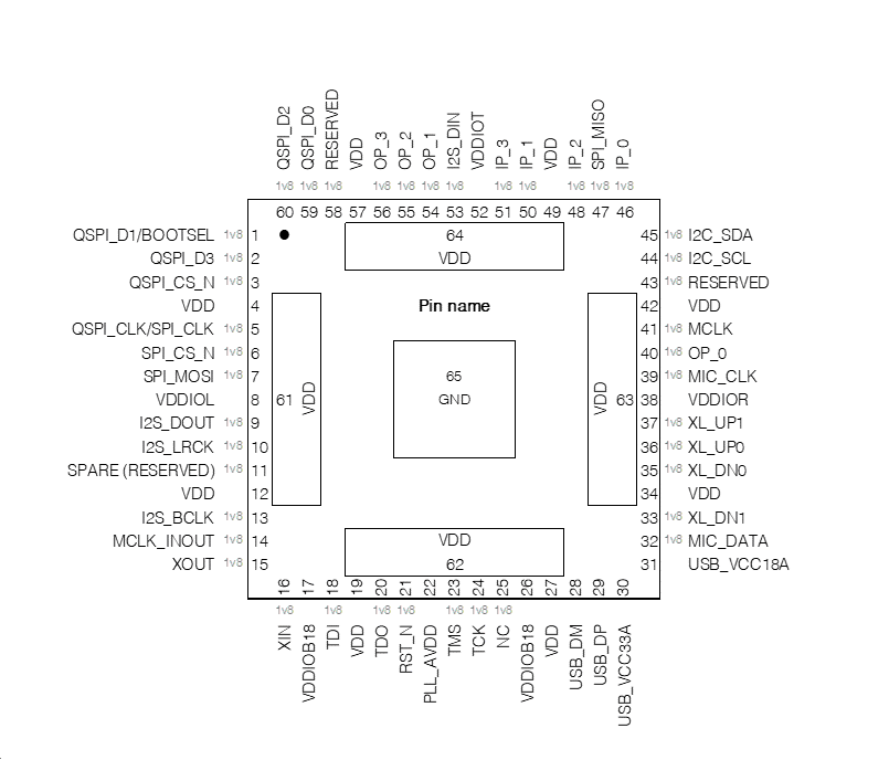
Fig. 12 XVF3610-QF60A pin configuration
Note
In both variants, VDDIO18 must be connected to a 1V8 supply and all VDD pins must be connected to a 0V9 supply. All package paddles (pins 61 to 65) must be connected. It is advised that vias be placed under paddles to connect directly to PCB supply planes
Signal description
The table below lists the functions of all the pins shown in Figure 2‑1 above in the order they appear around the package.
Note: The function of some pins changes depending on the firmware configuration loaded during boot (-INT/-UA).
Pin |
Port |
Signal |
Description |
Comments |
Direction |
Power rail |
|---|---|---|---|---|---|---|
1 |
X0D05 |
QSPI_D1/BOOTSEL |
QSPI Data Line 1 and boot selection. |
If pin is tied high via a 4.7k ohm resistor on startup, the device will start in SPI slave boot mode. If the pin is left floating, pulled low or connected to a quad SPI D1 pin on a memory device, the device will start in QSPI master mode and attempt to boot from a local QSPI flash memory. |
I / O |
IOL |
2 |
X0D07 |
QSPI_D3 |
QSPI Data Line 3 |
I / O |
IOL |
|
3 |
X0D01 |
QSPI_CS_N |
QSPI Boot Flash - Chip Select |
Pull high externally to the device using a 4.7k ohm resistor |
O |
IOL |
5 |
X0D10 |
QSPI_CLK/SPI_CLK |
QSPI Clock |
O |
IOL |
|
6 |
X0D00 |
SPI_CS_N |
Slave SPI boot / Peripheral SPI Master Chip Select |
Pull high externally to the device using a 4.7k ohm resistor |
I |
IOL |
7 |
X0D11 |
SPI_MOSI |
SPI Master Out Slave In |
I |
IOL |
|
8 |
VDDIOL |
VDDIOL |
I/O Power Supply (1v8) |
All VDD pins must be connected. |
PWR |
NA |
9 |
X1D00 |
I2S_DOUT |
I2S Data Out |
Audio data out to host processor |
O |
IOL |
10 |
X1D01 |
I2S_LRCK |
I2S Left/Right clock |
48kHz or 16KHz clock derived as I2S_BLCK/64. |
O (master), I (slave) |
IOL |
11 |
X1D09 |
SPARE (RESERVED) |
(blank) |
(blank) |
(blank) |
IOL |
13 |
X1D10 |
I2S_BCLK |
I2S bit synchronisation clock |
Configurable for 16KHz (1.024MHz) and 48KHz (3.072MHz) sample rates |
O (master), I (slave) |
IOL |
14 |
X1D11 |
MCLK_INOUT |
(blank) |
(blank) |
(blank) |
IOL |
15 |
XOUT |
XOUT |
Crystal oscillator output |
Note that this pin should be left floating when using the CMOS clock input |
O |
IOB |
16 |
XIN |
XIN |
Crystal oscillator input or CMOS clock input |
alternatively this can be used as a clock input |
I |
IOB |
18 |
TDI |
TDI |
JTAG test data input |
This pin has a weak internal pull-up. See note on debug headers. |
I |
IOB |
20 |
TDO |
TDO |
JTAG test data output |
See note on debug headers. |
O |
IOB |
21 |
RST_N |
RST_N |
Device reset |
Active low. This pin has a Schmitt trigger input and an internal weak pull up |
I |
IOB |
22 |
PLL_AVDD |
PLL_AVDD |
Analogue power supply for core and application PLL. |
Use a filtered version of the core supply, as per the XU316-1024-QF60A datasheet. |
PWR |
(blank) |
23 |
TMS |
TMS |
JTAG test mode select |
This pin has a weak internal pull-up. See note on debug headers.. |
I |
IOB |
24 |
TCK |
TCK |
JTAG test clock input |
This pin has a Schmitt trigger input and an internal weak pull-down. See note on debug headers. |
I |
IOB |
25 |
NC |
NC |
Not connected. This pin should NOT be connected to any net |
IOB |
||
28 |
USB_DM |
USB_DM |
USB D- line. May be left floating if USB is not required |
(blank) |
||
29 |
USB_DP |
USB_DP |
USB D+ line. May be left floating if USB is not required |
(blank) |
||
30 |
USB_VDD33A |
USB_VCC33A |
(blank) |
USB 3.3V power for the USB transceiver. May be left floating if USB is not required |
PWR |
(blank) |
31 |
USB_VDD18A |
USB_VCC18A |
(blank) |
USB 1.8V power for the USB transceiver. May be left floating if USB is not required |
PWR |
(blank) |
32 |
X1D13 |
MIC_DATA |
PDM microphone input |
Note that this is a DDR input, permitting a pair of digital DDR microphones to share this input |
I |
IOR |
33 |
X1D16 |
XL_DN1 |
XLINK |
These 4 signals form a single 2-wire xlink connection for advanced debug only. Do not connect in production desings. |
I |
IOR |
35 |
X1D17 |
XL_DN0 |
XLINK |
(blank) |
I |
IOR |
36 |
X1D18 |
XL_UP0 |
XLINK |
(blank) |
O |
IOR |
37 |
X1D19 |
XL_UP1 |
XLINK |
(blank) |
O |
IOR |
38 |
VDDIOR |
VDDIOR |
I/O Power Supply (1v8) |
All VDD pins must be connected. |
PWR |
NA |
39 |
X1D22 |
MIC_CLK |
Microphone clock output. |
3.072MHz |
O |
IOR |
40 |
X0D29 |
OP_0 |
General purpose output |
Eval kit - Used as interrupt to the RaPi, via an I2C expander. |
O |
IOR |
41 |
X0D35 |
MCLK |
Master audio clock |
I |
IOR |
|
43 |
X0D36 |
RESERVED |
(blank) |
Leave this pin unconnected |
I |
IOR |
44 |
X0D37 |
I2C_SCL |
I2C serial clock line for receiving control command from I2C host |
I / O |
IOR |
|
45 |
X0D38 |
I2C_SDA |
I2C serial data line for receiving control command from I2C host |
I / O |
IOR |
|
46 |
X0D40 |
IP_0 |
General purpose input |
I |
IOT |
|
47 |
X0D39 |
SPI_MISO |
SPI Master In Slave Out |
May be left floating if not required |
O |
IOT |
48 |
X0D42 |
IP_2 |
General purpose input |
I |
IOT |
|
50 |
X0D41 |
IP_1 |
General purpose input |
I |
IOT |
|
51 |
X0D43 |
IP_3 |
General purpose input |
I |
IOT |
|
52 |
VDDIOT |
VDDIOT |
I/O Power Supply (1v8) |
All VDD pins must be connected. |
PWR |
NA |
53 |
X1D34 |
I2S_DIN |
Peripheral I2S interface - I2S data input |
(blank) |
I |
IOT |
54 |
X0D30 |
OP_1 |
General purpose output |
Eval kit - LED_R |
O |
IOT |
55 |
X0D31 |
OP_2 |
General purpose output |
Eval kit - LED_G |
O |
IOT |
56 |
X0D32 |
OP_3 |
General purpose output |
Eval kit - Test point (and DAC reset if no-fit resistor fitted) |
O |
IOT |
58 |
X0D33 |
RESERVED |
(blank) |
Leave this pin unconnected |
(blank) |
IOT |
59 |
X0D04 |
QSPI_D0 |
QSPI Boot Flash, QSPI Data Line 0 |
I / O |
IOL |
|
60 |
X0D06 |
QSPI_D2 |
QSPI Data Line 2 |
I / O |
IOL |
|
65 |
GND |
GND |
Ground |
All package paddles must be connected. It is advised that vias be placed under paddles to connect directly to PCB supply planes |
GND |
NA |
17, 26 |
VDDIOB18 |
VDDIOB18 |
I/O Power Supply (1v8) |
All VDD pins must be connected. |
PWR |
NA |
4, 12, 19, 27, 34, 42, 49, 57, 61, 62, 63, 64 |
VDD |
VDD |
Core power supply (0v9) |
All package paddles must be connected. It is advised that vias be placed under paddles to connect directly to PCB supply planes |
PWR |
NA |
All VDD pins must be connected, excluding the USB_VDD supplies which can be left floating if USB is not required.
- Two package variants are available:QF60A – (1V8 I/0) – VDDIOT, VDDIOL and VDDIOR must be connected a 1V8 supplyQF60B – (3V3 I/0) – VDDIOT, VDDIOL and VDDIOR must be connected a 3V3 supply
In both variants, VDDIO18 must be connected to a 1V8 supply must be connected.
All package paddles must be connected. It is advised that vias be placed under paddles to connect directly to PCB supply planes