Device operation
Power supplies
The XVF3610 has the following power supply pins:
Name |
Description |
Pin |
|---|---|---|
VDD |
Digital core power supply. 0.9V (nominal) |
4, 12, 19, 27, 34, 42, 49, 57, 61-64 |
V DDIOL |
Digital I/O power supply ** See Note A. |
8 |
V DDIOR |
Digital I/O power supply ** See Note A |
38 |
V DDIOT |
Digital I/O power supply ** See Note A |
52 |
VDD IOB18 |
Digital I/O power supply. 1.8V (nominal) |
17,26 |
PLL _AVDD |
PLL analogue power. This 0.9V (nominal) PLL supply should be separated from the other supplies at the same voltage by a low pass filter. |
22 |
USB _ VDD18 |
Digital supply to the USB-PHY. 1.8V (nominal) |
31 |
USB _ VDD33 |
Analogue supply to the USB-PHY. 3.3V (nominal) |
30 |
VSS |
Device Ground |
65 (Paddle) |
Warning
A: I/O voltage depends on package variant
QF60A – VDDIOx is 1.8V nominal – pins 8, 38 and 52 should be connected to a 1.8V supply
QF60B – VDDIOx is 3.3V nominal – pins 8, 38 and 52 should be connected to a 3.3V supply
For both variants, VDDIOB18 – pins 17 & 26 - must be connected to 1.8V
B: All VDD power pins must be connected.
C: USB_VDDxx supplies can be left floating if USB is not used.
See also
The XU316-1024-QF60(A/B) datasheets contain further information on power supplies and power on sequencing.
Clocks
The XVF3610 device has an on-chip oscillator. To use the oscillator a crystal, two capacitors, and damping and feedback resistors to the device as shown below.
Signal |
Description |
Comment |
P in |
I /O |
|---|---|---|---|---|
XIN |
Crystal oscillator input |
16 |
I |
|
XOUT |
Crystal oscillator output |
15 |
O |
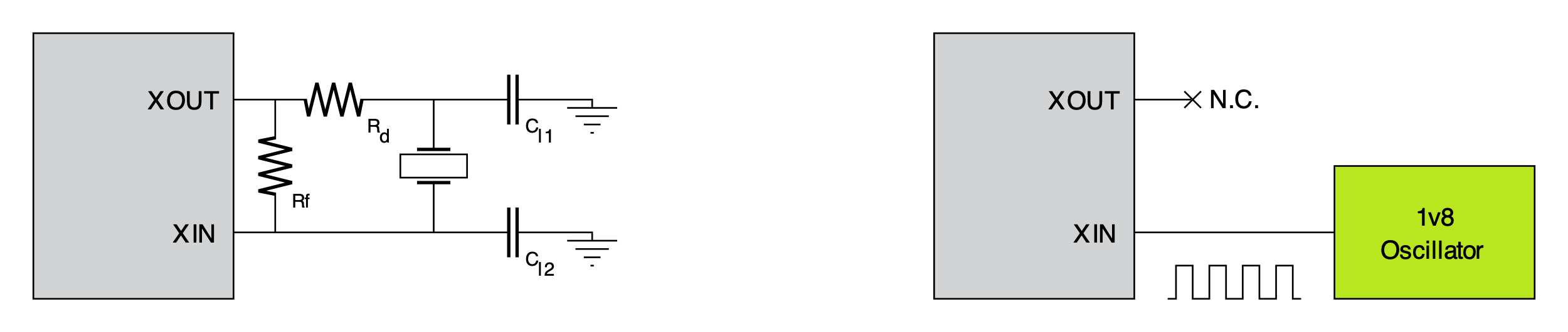
Fig. 15 Crystal oscillator or clock input configurations
Alternatively, the XVF3610 can be provided with a 24MHz, 1V8 clock input on the XIN pin. The clock must be running when the chip comes out of reset.
Signal |
Description |
Comment |
P in |
I /O |
|---|---|---|---|---|
XIN |
Master clock (system) |
24MHz 1V8 clock signal |
16 |
I |
XOUT |
N/C |
Leave floating if clock input on XIN |
15 |
O |
See also
For further information, and details on the calculation of Rf and Rd, please refer to the XU316-1024-QF60(A/B) datasheets.
Reset
The XVF3610 device has an on-chip Power-on-Reset (POR). This keeps the chip in reset whilst the supplies are coming up.
See XU316-1024-QF60(A/B) datasheet for further information.
Signal |
Description |
Comment |
P i n |
I - O |
|---|---|---|---|---|
RST_N |
Device reset |
Active low |
2 1 |
I |
Boot modes
On start-up and after a reset event, the XVF3610 is booted either using an externally connected QSPI flash memory or by transferring a boot image to the device via SPI from a host processor.
Slave boot mode
The boot mode is specified using QSPI_D1/BOOTSEL. If this pin is tied high via a 4.7k ohm resistor on start-up, the XVF3610 will enable SPI Slave boot mode and activate the pins shown below.
Signal |
Description |
Comment |
P i n |
I - O |
|---|---|---|---|---|
QSPI_C LK/SPI_CLK |
SPI Clock |
5 |
I |
|
SPI_CS_N |
SPI Chip Select |
Pull high externally to the device using a 4.7k ohm resistor. |
6 |
I |
SPI_MOSI |
SPI Master Out Slave In |
7 |
I |
|
SPI_MISO |
SPI Master In Slave Out |
4 7 |
O |
QSPI master boot mode
If the QSPI_D1/BOOTSEL pin is connected to a QSPI_D1 pin on a flash device, the XVF3610 will boot from a local QSPI flash in QSPI Master mode. The active pins are shown below.
Name |
Description |
P i n |
I - O |
|---|---|---|---|
QSPI_CS_N |
QSPI Chip Select. This pin should be pulled high externally to the device using a 4.7k ohm resistor. |
3 |
I - O |
QSPI_D0 |
QSPI Data Line 0 |
5 9 |
I - O |
QSPI_D1 - BOOTSEL |
QSPI Data Line 1 and boot selection. To activate QSPI master boot mode connect directly to QSPI Data Line 1 on Quad capable flash device. |
1 |
I - O |
QSPI_D2 |
QSPI Data Line 2 |
6 0 |
I - O |
QSPI_D3 |
QSPI Data Line 3 |
2 |
I - O |
QSPI_CLK / SPI_CLK |
QSPI Clock and SPI Clock |
5 |
I - O |
QSPI flash support
Flash devices with the following specifications are supported by the XVF3610 (eg. Winbond W25Q16JWSNIM).
Device characteristic |
Description |
Value |
|---|---|---|
Page size |
Size of flash page in bytes |
256 |
Number of pages |
Total number of pages |
8192 |
Address size |
Number of bytes used to represent the address |
3 |
Read ID operation code |
Operation code to read the device identification (ID) information |
0x9F |
Read ID dummy bytes |
Number of dummy bytes after read command before ID is returned |
0 |
ID size |
Size of ID in bytes |
3 |
Sector Erase operation code |
Operation code for 4 KB Erase |
0x20 |
Sector information |
Arrangement of sectors |
Regular (all equally sized - 4KB) |
Write Enable operation code |
Operation code for write enable |
0x06 |
Write Disable operation code |
Operation code for write disable |
0x04 |
Page Program operation code |
Operation code for page program |
0x02 |
Fast Quad Read operation code |
Operation code for Fast Quad I/O Read |
0xEB |
Fast Quad Read Dummy Bytes |
Number of dummy bytes after setup of fast quad read that data is returned |
1 |
Read Status Register operation code |
Operation code for reading status register |
0x05 |
Write Status Register operation code |
Operation code for write to the status register |
0x01 |
Write Status Register Busy Mask |
Bit mask for operation in progress (device busy) |
0x01 |
Device firmware
Device Firmware Upgrade (DFU) is supported for devices that have QSPI flash connected and loaded with a firmware image. If the DFU process fails, the boot process safely falls back to the factory image allowing the user to re-attempt the upgrade. Images loaded via DFU can also be removed allowing the device to revert to the factory image.
For further information on the operation of the DFU mechanism refer to the User Guide.