


My university degree was what they call a co-op course in the USA. Standing for “cooperative education,” this refers to a program that balances classroom theory with periods of practical, hands-on experience. There were two types of such courses in the UK. One type was called a “thin sandwich” because it involved short alternating 6-week periods in and out of college. The other type, which I was on, was called a “thick sandwich” because it involved longer periods. As I recall, we were in college for a year, out in industry for six months, back in college for another year, out in industry for a second six-month stint, and then back to college for a final year. This all seemed to take a long time at the time—but looking back it seems to have flown by.
My first period in industry was at a Rolls-Royce Aerospace facility in a town called Filton, which is located about 5.5 miles north of the city of Bristol. I had a wonderful time exploring Bristol, which is a beautiful and historic metropolis featuring many beautiful and historic public houses that sell beautiful glasses of historic scrumpy cider (a brew so potent that wise men quaff it only in small glasses—if only I’d been wise). Sad to relate, I never got to return to Bristol after finishing my training there, which is around 45 years ago as I pen these words.
The reason I mention this is that the company XMOS is based in Bristol. For the past few years, I’ve had an open invitation to visit them whenever I’m in the UK. The problem is that whenever I am in the UK, it’s to visit my dear old mom, and she won’t let me out of her sight.
Why am I waffling about XMOS? Well, suppose you wish to create a new device for use with the internet of things (IoT). You are going to require some sort of processor, and several options are available to you. For example, you could decide to use an off-the-shelf microcontroller unit (MCU) or application processor (AP) from one of the usual suspects.
The problem here is that the characteristics of the IoT suggest that you won’t be able to find an MCU or an AP that’s a perfect fit. Either it will have more features than you require, in which case you will end up paying for functions you will never use, or it won’t have every feature you desire, in which case you will have to augment your bill of materials (BOM) with one or more additional devices (frowny face).
Another option is to create a system-on-chip (SoC) device. This might contain one or more ARM processor cores along with a bunch of other intellectual property (IP) blocks. The upside is that this will result in a screamingly fast processing solution. The downside is that it will probably take you three or four years until tape-out and cost you anything up to $50M. There’s also the chance that, when you finally have your chip in your hand, the market to which you were targeting your product may have evolved in a direction that’s not compatible with your swanky new device (super frowny face).
Yet another option is to use a field-programmable gate array (FPGA), which is great if you have access to skilled hardware design engineers with expertise in FPGA design. The issue here is that these guys and gals are in short supply. I’m not sure as to the exact ratio, but I wouldn’t be surprised to hear that there are 100+ software developers for every FPGA designer. Actually, I wouldn’t be shocked if you told me the ratio was 1000-to-1.
All of which brings us back to the lads and lasses at XMOS with their XCORE devices. These are much more powerful than traditional MCUs, cheaper than APs, available off-the-shelf (unlike SoCs), and can be used by traditional software developers (unlike FPGAs).
I’ve written about XMOS before (see One Step Closer to Voice-Controlled Everything and Next-Gen Voice Interfaces for Smart Things and Loquacious Folks). As you may recall, XMOS is a fabless semiconductor company that develops multicore microcontrollers capable of concurrently executing real-time tasks, implementing extreme digital signal processing (DSP), artificial intelligence (AI), and machine learning (ML) applications, and also managing control flow. XMOS microcontrollers are distinguished by their totally deterministic (predictable) behavior.
The easiest way to wrap our brains around this is by means of a handy-dandy diagram like the one shown below.
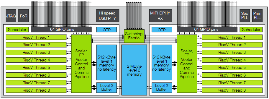
XCORE architecture (Source: XMOS)
We start with a tile, which has a scalar, floating-point (FP), vector, control and communications pipelined processor. This tile has its own local, tightly-coupled memory (not cache). Also associated with the tile are eight hardware threads. There are two such tiles on the device, each boasting 64 general-purpose input/output (GPIO) pins. These tiles can communicate with each other by means of a high-performance switching fabric. Observe that this switching fabric is also presented to the outside world (we will return to this point shortly).
One point that’s important to note is that the threads do not involve context switching in the traditional sense. These are hardware threads—each has its own register file, maintains its own state, and has its own access to the memory with guaranteed characteristics. Essentially, each thread has everything it needs to run autonomously; it just happens to be sharing the processing pipeline, but the way it shares this pipeline is entirely deterministic.
As I wrote in one of my earlier columns: “The XCORE architecture delivers, in hardware, many of the elements that are usually seen in a real-time operating system (RTOS). This includes the task scheduler, timers, I/O operations, and channel communication. By eliminating sources of timing uncertainty (interrupts, caches, buses, and other shared resources), XCORE devices can provide deterministic and predictable performance for many applications. A task can typically respond in nanoseconds to events such as external I/O or timers. This makes it possible to program XCORE devices to perform hard real-time tasks that would otherwise require dedicated hardware.”
If you look closely at the above diagram, you will see USB and MIPI PHYs (physical layers) but no USB or MIPI IP functional blocks (the PHYs provide the analog interface to the outside world). This is because all of the regular communications functions (like USB) and interface functions (like MIPI)—along with myriad other functions—are provided in the form of a software library, where each function ends up running on one or more of the hardware threads. This means developers can select the exact mix of functionality they require for their current project.
In addition to the XCORE architecture’s flexibility (everything is designed in software), and its determinacy (it acts like an RTOS implemented in hardware), one of the real differentiators is its scalability. If the developers decide they need more processing power in a future implementation of the product, they can simply add one or more XCORE chips linked by their externally presented switching fabric. A few years ago, as a proof-of-concept (PoC) to demonstrate this scalability, the folks at XMOS created a board called the XMP64, which featured an 8 x 8 array of XCORE chips, each with four tiles, and each tile with eight hardware threads. That’s like having 2,048 processors at your disposal (that distant “boom” you hear is my mind being blown).
Take one more look at the diagram above. Do you spot anything unexpected? Yes! You’ve got it! The hardware threads carry the RISC-V annotation. This is because the chaps and chapesses at XMOS recently announced that the next incarnation of their device, the 4th generation of the XCORE architecture, will be RISC-V compatible.
This is HUGE news. They had thought of doing this with their 3rd generation architecture but—at that time (circa 2017)—they felt the widespread adoption of RISC-V was not inevitable. The XMOS mission has always been to make using their device as normal as possible to ensure that the largest audience of developers can take full advantage of this technology. They now believe widespread RISC-V adoption is inevitable, which is why the new XCORE architecture is RISC-V compatible.
The end result of all this is that developers will be able to enjoy a familiar RISC-V experience employing familiar RISC-V tools while creating a highly differentiated outcome. These new RISC-V compatible XCORE devices are expected to become available later this year, and I—for one—cannot wait. What say you?


Could you please list a few “familiar” RISC-V tools?
“The end result of all this is that developers will be able to enjoy a familiar RISC-V experience employing familiar RISC-V tools while creating a highly differentiated outcome. “
Hi Karl — I will ask the folks at XMOS to dive in here.
The compilation chain we ship will be built on top of existing support for the RISC-V ISA by the LLVM project. That gives us C/C++ compilers, linker and assembler/disassembler which will be familiar and still support xcore extensions to the instruction set. There are also numerous simulation and debugging tools already out there for RISC-V targets.
Watch out for HLS/SystemC
I hear a lot of good things about HLS, but I also hear that it’s not quite as easy to use as one might hope (not exactly push-button, as it were).
Hi, Max. Here are some assignment expressions that I am using for debug. As simple as I can imagine. The main() is to get the compiler’s attention and really does nothing.
main()
z = 2 * 3 – 4 * 5;
A = 11 + 12 * 13 – (14 + 15) * 10;
X = 2 * 3 + 4 * 5;
y = y + 1;
x = 5 – 10;
B = 4 + 6 – 17;
y = 2 + 3 * 4 – 4;
X = 2 * 3 + 4 * 5;
y = 2 + 3 * 4 – 4;
y = 0;
y = 2 + 3 * 4 – 4;
y = y + 2;
y = y + 1;
X = 2 * 3 + 4 * 5;
A = 11 + 12 * 13 – (14 + 15) * 10;
y = y + 1;
I use the C# API to read, parse, and evaluate in debug mode with Visual Studio IDE. he secret sauce behind this is the compiler uses and Abstract Syntax Tree and stack based evaluation, something HLS probably never considered.
About as easy as I can imagine.
The compiler and Visual Studio are both free for open source usage and I will add my source code as open source if I ever figure out how.
Another project is evaluate conditional assignment expressions for Boolean expressions.
That might appeal to a man of your trade.
One more question. How many are there in the world who can program this thing?
Well, based on the fact that they have hundreds of companies using these devices, I’d say “quite a lot.” But again, I’ll ask the folks at XMOS to respond.
Hi, Max. My apology — I was thinking multi threading in traditional sense, but you already covered that.
But I do not see the need to share anything.
I chose to use an FPGA and it took 3 embedded memory blocks and a few hundred LUTs to implement a “thread” that is extremely fast because the memories are full dual port and having independent memories for each “thread” allows the memories to actually function as registers.
(this is the prototype that I cannot find and am busy creating a new design that is taking far too long)
I will keep plugging along.
“Here are some assignment expressions that I am using for debug.”
It seems to me that you are having too much fun LOL
Would love to see a modern microkernel OS written (in Rust) to take advantage of this, even if it’s running Linux in a container to gain adoption. Also would love SailfishOS phone running on this
I think you’ve just defined your next hobby project 🙂
No need for an OS. Does RUST use an AST? A compiler that uses an AST AND provides an API such as Roslyn does is enough.
I realize that Microsoft is a dirty word, but am here to tell everybody that C# compiler API that includes a “SyntaxWalker” is very useful.
Oh, but it uses a stack and a stack can overflow is a common reply…so what? every compiler uses a stack and usually allocates memory from the stack. My design uses a memory block for a stack and no harm is done if it overflows(except that it is a bug)